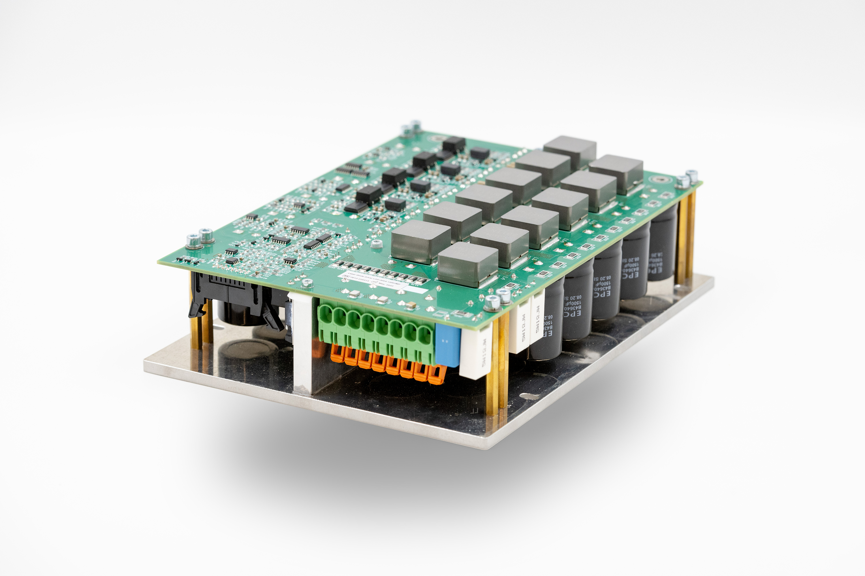
< Back to laser diode drivers

LDD-300A-120V-IMP

High power open-board type pulsed laser diode driver LDD-300A-120V-IMP

300A
Pulsed
150V
Voltage
<25µs
Rise/Fall
Request Price Request Price

Description

The laser diode driver (LDD) is designed to feed a laser diode with a desired pulsed current (QCW mode). It is an open board type DC/DC converter and is designed for OEM integration. Requires dedicated AC/DC power supply.

Specification

Description

Testing conditions:

MIN

AVG

MAX

Units

OUTPUT

Output current (IOUT)

Fig. 3...12


300

A

Maximum output voltage (VOUT)

IOUT = 300A

VIN –7


V

Current rise/fall when controlled via the IN_MOD input

60A < IOUT < 300A,
0.1Ohm < RLOAD < 0.4Ohm,
VOUT < VIN –35V


15

25

µs

Current rise/fall when controlled by the IPROG step voltage

60A < IOUT < 300A,
0.1Ohm < RLOAD < 0.4Ohm,
VOUT < VIN –35V


200


µs

INPUT

Input current without load

100V < VIN < 155V


0.15

A

Threshold input (VIN) breakover voltage


65

V

Efficiency

IOUT = 300A, VOUT = 120V,
VIN = 150V, tPꞏFP > 0.01

85


%

Input capacitance

LDD-300A-120V-IMP

LDD-300A-120V-IMP-CAP


42,000

100,500


µF

ANALOG SIGNALS

Output current to the IPROG – GNDA voltage ratio


30


A/V

Output current setting error by the IPROG signal

IOUT = 300A

IOUT = 60A


1

2

%

The IMON – GNDA voltage
 to output current ratio


0.0333


V/A

Output current control error

IOUT = 300A

IOUT = 60A


1

2

%

The VMON – GNDA voltage
 to output voltage ratio


0.04


V/V

Output voltage control error

VOUT > 40V


1

%

DISCRETE SIGNALS

High level signal at IN_MODE, ENABLE inputs


2


V

Low level signal at IN_MODE, ENABLE inputs


0.8

V

Input sink current IN_MOD

VIN_MOD = 5V


4.5


mA

Input sink current ENABLE

VENABLE = 5V


0.25


mA

Threshold level signal at the INTLOCK input


1.2


V

Input source current INTLOCK

VINTLOCK = 0


0.35


mA

Start delay by the ENABLE, INTLOCK signals

VENABLE > 3V,
VINTLOCK < 0.5V


100

µs

Stop delay by the ENABLE, INTLOCK signals

VENABLE < 0.5V


30

µs

OUTPUT +15VPI

Output voltage

Load current I+15VPI = 0


15


V

Output resistance


10


Ohm

Signals

Output current

Overall dimensions

Production facility

Astrum LT s.r.o. is a brand-new semiconductor laser production facility, located in Czech Republic, Kralupy nad Vltavou (Prague area).

OEM laser solutions for medical, industrial, automotive, semiconductor and consumer electronic applications.

Our most valuable benefits of our laser solutions

Most valuable benefits of our laser solutions

Accuracy

Accuracy

Quality

Quality

Safety

Safety

Precise design

Precise design

Sustainability

Sustainability

Durability

Durability

State-of-the-art semiconductor laser production facility

Located in Czech Republic, Kralupy nad Vltavou the fab offers 6,000m² of total engineering area, including 2,000m² of clean room.

Registered office Registered office:
U Dýhárny 1177,
27801 Kralupy nad Vltavou,
Czech republic
2,000m²
Clean room