ASTRUM LT offers CONTRACT R&D:
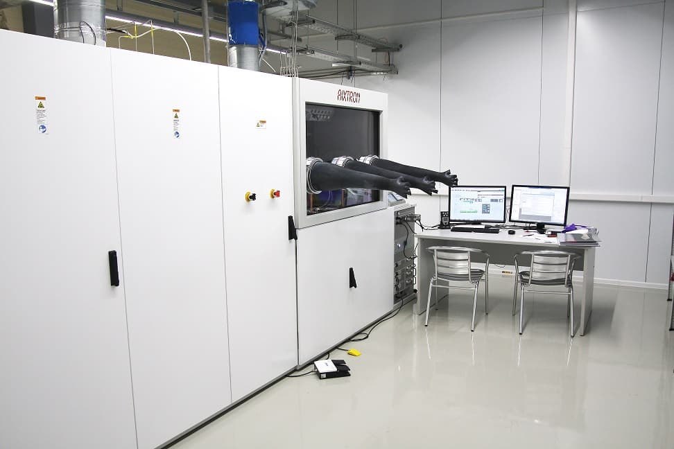
CUSTOM MOCVD EPITAXY
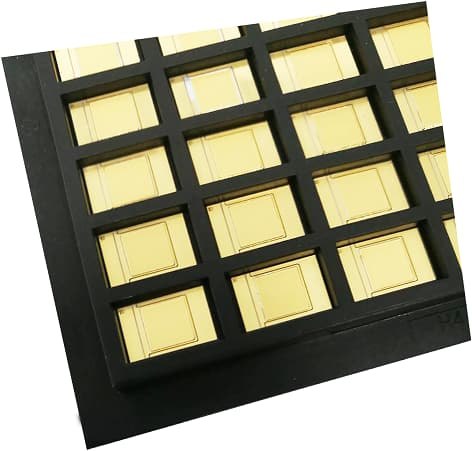
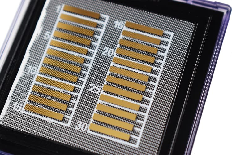
CUSTOM LASER DIODE BARS
Custom wavelength
CW or QCW, up to 200W
MOCVD technology offers a number of advantages:
- Exceptionally high quality of layers: higher growth rate at high doping uniformity and consistency.
- High yield: no need for ultra-high vacuum allows for better up-time.
- Flexibility: growth of various materials and during the same process run.
- Growth of multi quantum wells structures (MQW structures).
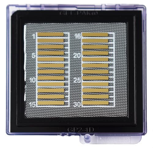
CUSTOM LASER DIODE BARS
Custom wavelength
CW or QCW, up to 200W
MOCVD CAPABILITIES
AlGaInP/GaAs LED, lasers 635 – 780nm automotive industry, street lights, DVD, displays
AlGaAs/GaAs lasers 780 – 1060nm CD, telecommunication, high power lasers
AlInAs/GaInAs/InP LED, lasers 1300 – 1600nm IR - diodes, high power optical modules
MOCVD CAPACITIES
AIXTRON with configurations of 2", 3", or 4” wafers
Doping concentration from 1E13cm-3 to 1E20cm-3
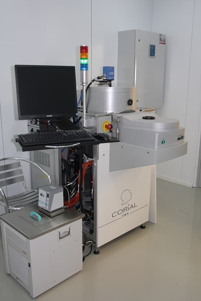
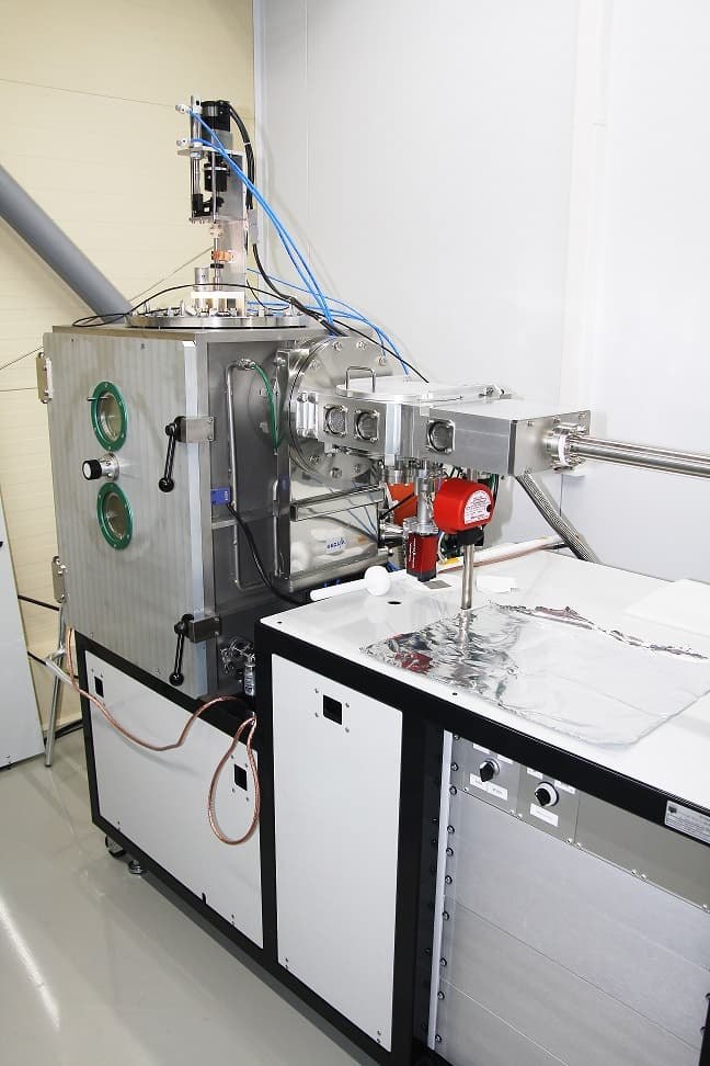
IN-HOUSE MOCVD CHARACTERIZATION
Surface defects mapping
X-ray diffraction
ECV profiling
Wafer photoluminescence (PL) mapping
Scanning Electron Microscopy (SEM)